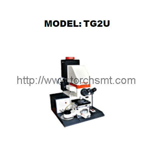
Chip Checking Microscope TG2U
- Technical Data Sheet
Introduction:
TG2U lithography is used in the LSI, sensor, surface wave component, magnetic bubble, microwave, CCD and so on.
Remark:
1. Template size:
a. 100×100×2-3mm;
b. 75×75×2-3mm;
2. silicon size: Φ50-Φ75mm, real line width 3-4цm;
3. comparative displacement between template and silicon:
a. X,Y ≥±2. 5mm;
b. θ(rotate)≥±5°;
4. support station (silicon) rotate Z axies: rough tuning 360°, fine tuning ±5;
5. Integrated moving range of working station:X,Y integrate Φ75mm;
6. the space between ball basical station and template:0-7mm;
7. exposure system:GCQ200W over high-pressure ball Hg, exposure wave length:300~436nm;
8. engergy is not less than 407nm of wave length;7mw/cm;
9. uneven is within Φ75mm: ±5%:
10. lighting wave length: ≈545nm;
11. exposure time: O.01 seconds-99. 99 minutes;
12. the focusing range of binocular: 13mm;
13. the zoom of binocular;
a. pair ocular: lOX,16X;
b. flat field objective: 6X,9X,15X;
c. total zoom out: 60X-240X;
14. vacuum touching pressure: ≥O. 7Kgf;
15. power supply;
a. frequency: 50HZ(Z);
b. rotated input voltage: 190V-230V;
c. power consumption: ≤300VA;
16. Dimension: 1000X850X980mm (2 boxes)
17. Weight: ≈200Kg;
(1) vacuum supply: ≥450mm Hg;
(2) The device of air supply stability is below.
Add: If the user had any special request, please contact with us.