Date: 2019-12-27
This paper respectively from the IGBT chip structure, the structure of the collector area on the back and front MOS structure, the system analyzes the technology present situation and the characteristics of high power IGBT chip, from two aspects of chip welding and the electrode interconnection comprehensive IGBT module encapsulation technology is introduced, and the new structure, new technology and new materials technology three aspects analyzes the IGBT technology the development direction of the future.
Insulated Gate Bipolar Transistor (Insulated Gate Bipolar Transistor, the IGBT) is in the metal oxide field effect Transistor (MOSFET) and Bipolar Transistor (Bipolar) developed on the basis of a new type of composite power device, with functions of MOS input and Bipolar output.
IGBT has the advantages of low voltage drop, high current density, high voltage resistance and low power MOSFET drive power, fast switching speed, high input impedance and good thermal stability.
As the core device of power electronic converter, it lays a foundation for high frequency, miniaturization, high performance and high reliability of application device.
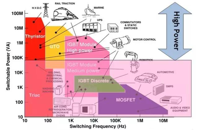
Since the commercial application of IGBT, as the main type of new power semiconductor devices, IGBT occupies an important position in the frequency application range of 1-100khz, with a voltage range of 600V -- 6500V and a current range of 1A -- 3600A(140mm x 190mm module).
IGBT is widely used in industries, 4C(communications, computers, consumer electronics, automotive electronics), aerospace, defense and other traditional industries, as well as rail transit, new energy, smart grid, new energy vehicles and other strategic emerging industries.
Adopting IGBT for power transformation can improve the efficiency and quality of electricity use, and it has the characteristics of high efficiency, energy saving and green environment protection. It is the key supporting technology to solve the problem of energy shortage and reduce carbon emission. Therefore, it is called "CPU" of power converter products and "core of green economy".
In a long period of time in the future, IGBT will play a more important role in meeting the strategic needs of global CO2 emission reduction, and will be an important fulcrum of energy-saving technology and low-carbon economy.
At present, the world's high-power semiconductor companies to IGBT research and development boom, research and technological innovation is increasingly accelerated, IGBT chip design and production manufacturers are Infineon, ABB, Mitsubishi Electric, Dynex(China south car, CSR), IXYS Corporation, International Rectifier, Powerex, Philips, Motorola, Fuji Electric, Hitachi, Toshiba, etc., mainly concentrated in Europe, America, Japan and other countries.
For a variety of reasons, although domestic IGBT technology research and development started early, but the progress is slow, especially in the industrialization of IGBT is still in the initial stage, as the world's largest IGBT application market, IGBT module mainly relies on imports.
In recent years, under the guidance and organization of national macro policy, domestic enterprises through various channels in IGBT chips, modules, and other fields has made a lot of gratifying progress, British Dynex semiconductor CSR through m&a, make full use of the European rich technical resources, set up overseas r&d center power semiconductors, quickly mastered the advanced 1200 v to 6500 v IGBT chip design, manufacture process and module encapsulation technology, and in zhuzhou, building an advanced 8 inches IGBT chip encapsulation production line.
The IGBT chip will be mass produced in early 2014.
The IGBT vacuum eutectic furnace, produced by TORCH, powers IGBT factories and adds bricks and mortar to IGBT products made in China with professional technology and technology.
In terms of module packaging technology, China has basically mastered the traditional welding packaging technology, among which there are many medium and low voltage IGBT module packaging manufacturers, while the high voltage IGBT module packaging mainly focuses on CSR and CNR.
The technology gap remains with foreign companies.
Based on the traditional packaging technology, foreign companies have developed a variety of advanced packaging technology, which can greatly improve the power density, heat dissipation performance and long-term reliability of the module, and initially realized the commercial application.
TORCH comrade IGBT vacuum packaging technology has been in BYD and other large IGBT companies through long-term verification.
2 technical status
2.1 IGBT chip technology
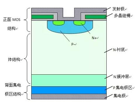
IGBT (vacuum eutectic furnace) chip is structurally composed of tens of thousands of cells (repetitive units), and is manufactured by lsi technology and power device technology [2].
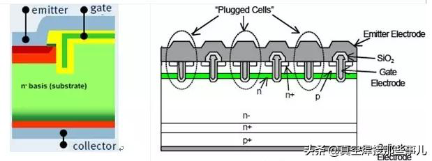
The structure of each cell is shown in figure 2 below, which can be divided into three parts: body structure, front MOS structure and back collector region structure.
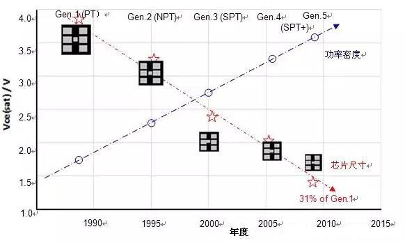
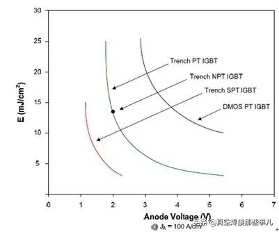
The development of volume structure design technology for commercial IGBT has gone Through a process from Punch Through (PT) to Non Punch Through (NPT) and then to Soft Punch Through (SPT), as shown in figure 3 [3].
Before the through-through structure, the bulk structure of IGBT was a non-through-through structure based on the thick wafer diffusion process, and the injection efficiency of the back hole was very high. Due to the parasitic thyristor structure inside the device, IGBT was prone to latch when working, so it was difficult to realize commercial use.
With the development of epitaxial technology, the n-type buffer layer was introduced to form a penetrating structure, which reduced the injection efficiency of holes in the back and realized batch application. However, due to the characteristics of epitaxial technology, the development of high voltage IGBT was limited, and its highest voltage level was 1700V.
With the development of zonal thin wafer technology, non-pass-through structure IGBT based on n-type substrates promotes the continuous improvement of the voltage level, and IGBT has a positive temperature coefficient through hole injection efficiency control technology, which can better realize parallel application and improve the application power level.
With increasing voltage level, the chip substrate thickness also increases rapidly, and eventually lead to state pressure drop increases, in order to optimize the state the pressure drop and pressure, the relationship between local Through structure arises at the historic moment, ABB is called Soft Through (Soft Punch Through, SPT) [4], infineon is called the electric Field as (Field Stop, FS) [5], mitsubishi called weak Through (Light Punch Through, LPT) [6].
IXYS call it eXtremely light Punch Through (XPT), as well as other names such as Thin Punch Through (TPT) and Controlled Punch Through (CPT)[7].
Under the same pressure resistance, the thickness of the soft-through-through structure is 30% lower than that of the non-through-through structure, while maintaining the positive temperature coefficient of the non-through-through structure.
In recent years, various enhanced technologies and ultra-thin chip technologies are based on the body structure of soft-through-through. Currently, the thickness of 600V voltage grade soft-through-through IGBT chip can reach 70um.
The collector structure of IGBT affects the gain of PNP transistor and has important influence on forward voltage drop and turn-off loss.
The early penetrating type IGBT had a large junction depth in the collector area and a large hole injection efficiency, which was prone to latch effect. Therefore, local life control technology must be adopted to control the back hole injection efficiency, but the negative temperature coefficient of conduction pressure drop resulted from the surface, which was not conducive to parallel application.
The later non-penetrating IGBT, with a transparent collector structure.
The hole injection is controlled, local life control is eliminated, and the positive temperature coefficient of conduction pressure drop is realized. This structural technique has been used to this day and has been optimized to improve the shut-off speed and short-circuit safe working area characteristics.
In view of the difficulty in processing chips with a voltage of less than 1200V due to the chip thickness, an "inner transparent collector" structure is proposed, which USES the method of helium ion implantation and epitaxy to avoid the ultra-thin chip processing technology to form a transparent collector.
The collector structure also has an important influence on the characteristics of the safe working area, especially the short-circuit safe working area. For applications with special requirements on the characteristics of the short-circuit safe working area, the compromise between the off loss and the doping concentration of the collector area and the injection efficiency of the buffer layer can be achieved by controlling and optimizing the doping concentration of the collector area and the injection efficiency of the buffer layer.
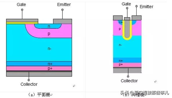
The front MOS structure of IGBT includes gate and emitter regions.
The grid structure has two types: plane gate (FIG. 4(a)) and groove gate (FIG. 4(b)).
The planar gate structure has a good quality of the gate oxide layer, and its gate capacitance is small, and it will not cause electric field concentration at the bottom of the gate and affect the withstand voltage. Therefore, it is widely used in high voltage IGBT(voltage class of 3300V and above).
Through optimization and improvement of planar gate structure, gate capacitance can be further reduced and other operating characteristics can be improved, such as reducing gate storage time, reducing switching loss, and reducing gate voltage overvoltage in short circuit safe working area (SCSOA) test [16].
Will channel and grooved gate structure from horizontal to vertical, eliminate the effect of the conduction resistance RJFET, also can improve the cellular density, thus to reduce the power consumption [17], therefore they are widely used in low voltage (1700 v) and under voltage grade product, but the groove etching after rough surface, can cause electric field concentration, carrier mobility and affect the breakdown voltage, and polysilicon gate area increase, make gate capacitance increases, in addition, due to the current density results in the decrease of the short circuit capacity.
In order to reduce the gate capacitance and reduce the short-circuit current, it is necessary to optimize the cellular structure, as shown in figure 5.
Mitsubishi proposed a "cellular combined" IGBT structure (plugged/dummy cells)[18-19](FIG. 6) to reduce saturation current, improve short-circuit capability, and suppress gate voltage oscillation during short-circuit testing.
In order to meet different packaging needs, IGBT gate electrode can be located in the center of the chip, the center of the edge and the corner, for the welding package, these three positions can meet the requirements, for the compression package, generally choose to set the gate electrode at the corner.
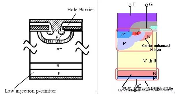
Currently, the advanced enhancement technology is to improve the electron injection efficiency at the end near the emitter region by optimizing the MOS structure on the front side, so as to optimize the tradeoff relationship between on-off pressure drop and turn-off loss (figure 7).
The Carrier storage Layer (CSL)/ Hole Barrier Layer (HBL) structure is commonly used, as shown in figure 8.
As can be seen from the figure, the structure surrounds the p-well by setting an n-type doped region on the periphery of the p-well.
The doped region shortens the channel length, and increases the hole carrier flows of barrier to the IGBT emitter, thus in the P - trap formed a hole accumulation layer, and increased in the condition of conduction electrons from the efficiency of the injection of MOS channel, enhances its conductivity modulation effect, can significantly reduce the conduction loss of the device.
In the realization of the process, the self - aligned process can be used, without increasing the number of lithography.
However, it is found that the n-doped region under the p-trap is not good for the voltage resistance of the chip.
In order to achieve a better compromise between on-off voltage drop and blocking voltage, the n-type doping technique beside the p-well was developed, that is, a pair of symmetric n-doped regions were formed on both sides of the p-well, as shown in figure 9 [23].
Compared with the carrier memory layer/hole barrier structure technology, the difference is that the doped region does not surround the bottom and corner of the p-trap, thus effectively reducing the on-chip voltage drop while maintaining the chip's voltage resistance to the greatest extent.
Other enhancement measures include optimizing the cellular structure of the groove or using special groove structure to reduce the efficiency of hole extraction in the base region, so as to achieve the purpose of electron injection enhancement, and to reduce the conduction loss while maintaining a low turn-off loss.
IGBT, IGBT vacuum welding furnace, IGBT vacuum eutectic furnace, IGBT vacuum reflow soldering, tin-tin soldering, Au80Sn20 welding, Au88Ge12, pre-set tin-tin cover, indium alloy solder sheet, tin-silver copper SAC solder sheet, lead-free solder sheet, Ag72Cu28, In52Sn48, indium silver alloy solder sheet, Sn90Sb10, Sn63Pb37, tin-lead solder sheet, gold-base solder sheet, silver based solder, indium, gold germanium solder, solder jinxi solder encapsulation, jinxi, IGBT high clean solder welding, pre - coating flux welding pieces, filling prefabricated by welding, soldering, SMT Ag92.5 Cu7.5 welding, Bi58Sn42 welding pieces, Pb60In40 welding pieces, In60Pb40 welding pieces, Pb75In25 welding piece, In50Sn50 welding piece, low temperature soldering, tin, pills, Zn95Al4Cu1 welding pieces, In51Bi32. 5 sn16. 5 welding pieces, In66.3 Bi33.7 welding, Ag62Sn35Pb3 welding pills
Ag60Cu23Sn17 Solder Preforms, Fluxless Solder, Solder ribbon
If you are interested in our products, please visit our website (www.torch.cc) or search IGBT vacuum welding oven on baidu to learn about our products.