Date: 2019-12-24
Toshiba is building high-level flash memory and ReRAM chips, and prototype samples are expected to be launched next year.
The idea of a high-rise or 3D chip is that we can bypass the limitations of the increased density of flash or memory chips and stack them up to increase the storage density, just as a high-rise house can accommodate more people.
According to Nikkei Electronics, Toshiba is building 3D stacks using an NAND, its p-bics technology, and ReRAM(resistive RAM), a potential alternative to NAND that combines RAM and NAND properties to provide byte addressing capability, DRAM level speed, and NAND non-volatility.
As shown in the figure below, the 3D flash contains the NAND stack layer, which is linked to the stack-based stack controller Via a communication hole (TSV or Through Silicon Via).
Instead of stacking the NAND chip on top of another chip, you stack the NAND layer on top of a single chip.
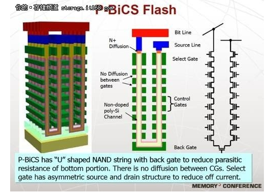
Toshiba p-bics technology
Toshiba's p-bics NAND has a 50-nanometer hole and 16 layers, and Masaki Momodomi, Toshiba's chief engineer, says p-bics is cheaper than the regular NAND when using more than 15 layers, assuming a similar capacity level.
The company plans to provide 128Gbit and 256Gbit prototype samples next year, engineering samples in 2014, and mass production in 2015. We'll have to wait another two years before we see the product on the market.
ReRAM technology is a similar schedule.
It has faster write times than NAND, Toshiba thinks ReRAM can play a different role from p-bics, it will be used to be closer to the unknown CPU than p-bics, and stt-ram is used for caching in SSDS.
Jim Handy of Objective Analysis said, "ReRAM will be used for high-performance applications that write faster than NAND, that are random-access devices that NAND is not, that don't require ECC, and that can lead to faster performance."
Prototype samples, engineering samples and mass production time of Toshiba's ReRAM technology will be basically consistent with p-bics.
Toshiba showed pictures of the 64Gbit ReRAM device, but Toshiba plans to provide a significant amount of p-bics and ReRAM.
Toshiba plans to reduce the size of its existing 1Xnm(19 nm)NAND unit, launching 1Ynm this year (18-14 nm to our knowledge) and 1Znm(10-13 nm) next year.
Handy said: "all of these new technologies (MRAM, ReRAM, FRAM, etc.) perform better than NAND (BiCS is a type of NAND), but are more expensive.
Cost is everything when it comes to memory, and these alternatives don't do that well.
"The promise of these technologies is that they will be able to scale past the limitations of NAND, and if that is the case, they will eventually be cheaper than NAND."
"Toshiba talked about 1y and 1z, 19 nanometers after the process.
I suspect NAND will stop expanding at about 10 nanometers, but BiCS will cause NAND prices to continue to fall."
Will we continue to see NAND size decline?
Or get more capacity from NAND's stack in 3D?
Handy said, "the latest ITRS(international semiconductor technology development roadmap) points NAND in two different directions, vertical (BiCS) and traditional.
The industry really doesn't know what the future holds, but let's see."
This article is from the network, if there is infringement, please contact me to delete